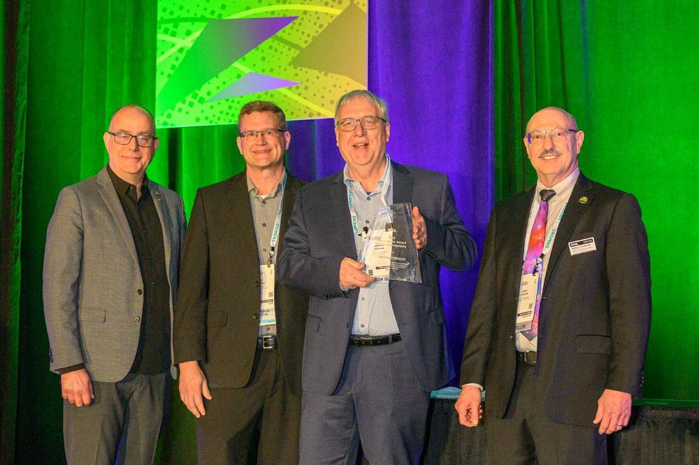
Andreas Erdmann is a senior expert in optical and EUV lithography with more than 30 years in the field. In 1999, he established the Computational Lithography and Optics group at the Fraunhofer Institute for Integrated Systems and Device Technology IISB in Erlangen, Germany, and led it until the end of 2025. Now, he continues to contribute to selected research projects at the institute and teaches at the Friedrich-Alexander-University Erlangen-Nuremberg, where he is involved as mentor of the Graduate School in Advanced Optical Technologies (SAOT). With the Frits Zernike Award 2026, his contributions to the understanding and modeling of image formation and resist patterning in DUV and EUV lithography, especially photomask’s 3D effects, and his commitment to lithography education, are honored.
Erdmann received the Frits Zernike award for his contributions to the understanding and modeling of image formation and resist patterning in deep and EUV lithography, especially photomask’s 3D effects, and for lithography education. »It has been my pleasure to have known Andreas for almost 30 years as a researcher in lithography simulation and later as a colleague, providing me direct insight into his contributions to the field«, says Nikon Research Corporation of America President, CEO, and COO Donis G. Flagello, who received the SPIE Frits Zernike Award for Microlithography in 2017.
»Professor Erdmann has made foundational contributions to computational lithography that have advanced micro- and nano-fabrication capabilities. His leadership in developing simulation platforms like Fraunhofer IISB’s Dr.LiTHO has enabled researchers and engineers to design and optimize lithographic processes, while his current work on wave coupling and waveguiding in low-n absorber materials for EUV, and exploration of machine learning and physics-informed neural networks for lithography modeling, demonstrates continued innovation. Professor Erdmann’s contributions, specifically to computational lithography have been instrumental to the advancement and knowledge base in our industry, and his work has illuminated complex optical phenomena and provided simulation capabilities that support each successive technology node development. But Professor Erdmann’s impact extends beyond individual research: He has mentored 16 PhD students and 23 Master’s students, and regularly delivers university lectures and conference courses, disseminating knowledge to the global community.«
A unique career in applied optics, dedicated to DUV and EUV lithography
While lithography simulation became his passion, Andreas Erdmann also focused on holography, nonlinear optics, guided wave optics, and modeling of optical systems. His work in lithography modeling has been particularly meritorious. Erdmann’s achievements include developing rigorous electromagnetic methods for accurate modeling of light diffraction from small features on DUV and EUV masks, elucidating the 3D effects of the EUV mask and their roles in image formation. He and his team also revealed the importance of wave coupling and waveguiding effects in low-refractive index (low-n) absorber materials and other mechanisms in EUV lithography. The theoretical framework and simulation tools have been key to the optimization of masks in DUV and EUV lithography.
Erdmann has shared his findings with the community in more than 330 conference and workshop presentations, including several invited and keynote talks, as well as over 200 scientific publications, such as papers in various SPIE journals and SPIE proceedings. Particularly noteworthy is the 2021 SPIE Press book Optical and EUV Lithography: A Modeling Perspective, educating many young engineers entering the field of semiconductor lithography. Erdmann contributed to the development of several advanced lithography simulators, above all the Dr. LiTHO simulator. He also served as conference chair and program committee member for multiple SPIE conferences such as Advanced Lithography + Patterning and Optical Systems Design. In addition, Erdmann is a reviewer for the SPIE journals Optical Engineering and Journal of Micro/Nanopatterning, Materials and Metrology. For the latter, he is also an Associate Editor in the Editorial Board.
In 2016, Andreas Erdmann was named a SPIE Fellow for his contributions to the field of optical and EUV lithography modeling. The title recognizes outstanding scientific and technological work in the fields of optics, photonics, and imaging. In addition, SPIE Fellows are distinguished by their above-average commitment to the scientific community in the field of optics and also to SPIE. Erdmann’s dedication to his students at the institute and the university has made him a committed and prolific educator. Many of his former students now work at major semiconductor companies.
SPIE Frits Zernike Award for Microlithography
The SPIE Frits Zernike Award for Microlithography is presented for outstanding accomplishments in microlithographic technology, especially those furthering the development of semiconductor lithographic imaging and patterning solutions. Frits Zernike (1888 – 1966) was a Dutch chemist, physicist, and mathematician who won the Nobel Prize for physics in 1953 for his invention of the phase-contrast microscope. Erdmann is the 23rd recipient of the award. Previously, the SPIE Frits Zernike Award for Microlithography had only been awarded to one German recipient, Winfried Kaiser from ZEISS in 2020.
About SPIE
SPIE is the international society for optics and photonics based in Bellingham, Washington, USA, founded in 1955 with members from over 180 countries. The main purpose of the organization is to strengthen the global optics and photonics community through conferences, publications, and professional development, bringing together engineers, scientists, students, and industry leaders to advance light-based science and technologies
The Fraunhofer Institute for Integrated Systems and Device Technology IISB is one of Europe’s leading research institutions for wide-bandgap semiconductors and power electronics, covering the complete value chain. The spectrum ranges from basic materials, semiconductor devices and process technologies, power electronic modules and components to complex power electronic and energy systems.
Main target applications of the IISB are semiconductor manufacturing, electromobility, aerospace, sustainable energy supply as well as civil security. With its solutions, the institute has been setting benchmarks in energy efficiency and performance, even for extreme operating conditions. The integration of intelligent data-based functionalities also continuously opens up new application scenarios. This allows the IISB to support customers and partners worldwide in transferring scientific results into commercial products.
A total of around 400 employees work at the IISB’s locations: the headquarters in Erlangen, the Cleantech Innovation Park in Hallstadt, and the Fraunhofer Technology Center High Performance Materials THM in Freiberg.
Fraunhofer-Institut für Integrierte Systeme und Bauelementetechnologie IISB
Schottkystraße 10
91058 Erlangen
Telefon: +49 (9131) 761-0
Telefax: +49 (9131) 761-390
http://www.iisb.fraunhofer.de
Computational Lithography and Optics
Telefon: +49 (1511) 6005601
E-Mail: andreas.erdmann@iisb.fraunhofer.de
![]()