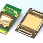
Avalanche-Photodioden-Array (APD) mit integriertem Self-Bias-Generator für den industriellen LiDAR-Einsatz
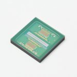
Wir, bei HAMAMATSU PHOTONICS, haben erfolgreich ein Avalanche-Photodioden-Array (APD) mit der Bezeichnung "Gain Stabilized Si APD S16430-01CR" für den industriellen LiDAR-Einsatz (*1) entwickelt. Dieses APD-Array wurde mit einem Self-Bias-Generator (SBG) (*2) integriert, indem wir unsere einzigartige, fortschrittliche Opto-Halbleiter-Fertigungstechnologie nutzten. Da Mehr