“The distinguishing characteristic of the project is to bring together technology and market experts, jointly defining technology roadmaps starting from application needs.” says Dr Patrick Cogez from AENEAS and industrial co-leader of the project. Following this approach, a series of workshops has involved more than 100 international research and application experts, coming from various institutions out of eleven countries.
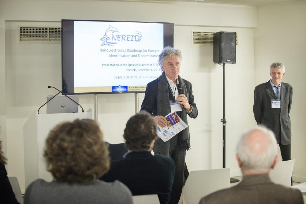
“The objective of NEREID is to elaborate a new roadmap for nanoelectronics, focused on the requirements of European semiconductor and application industries.” says Dr Francis Balestra from Grenoble INP and coordinator of the project. “It will address societal challenges following advanced concepts developed by Research Centres and Universities in order to achieve an early identification of promising novel technologies covering the R&D needs all along the innovation chain. The final result will be a roadmap for European micro- and nanoelectronics, with a clear identification of objectives from medium to long term.”
The NEREID roadmap for nanoelectronics is intended as input for future research programmes at European and National levels. It aims to help coordinating efforts to solve the main challenges in nanoelectronics and put the EU at the forefront of future technological developments. Therefore it takes into account the specificity of the European industrial and academic landscape, and targets a better coordination between academic and industrial research in equipment, semiconductors and application developments.
The NEREID roadmap is divided into several main technology sectors: Advanced Logic (including Nanoscale FETs and Memories) and Connectivity, Functional Diversification (Smart Sensors, Smart Energy, Energy for Autonomous Systems), Beyond-CMOS (Emerging Devices and Computing Paradigms), Heterogeneous Integration and System Design, Equipment, Materials and Manufacturing Science, and it also includes cross-functional enabling domains.
About the NEREID Project
NEREID is a three year Cooperation and Support action that has received funding from the European Union’s Horizon 2020 research and innovation programme under grant agreement No 685559, with the objective to develop a roadmap for the European Nanoelectronics industry, starting from the needs of applications and leveraging the strengths of the European eco-system. In addition, it will aim to an early benchmark/identification of promising novel nanoelectronic technologies, and identify bottlenecks all along the innovation value chain.
Highlights of the NEREID project, are three general workshops aiming at gathering the needs of the main application sectors, and specific workshops that define the roadmaps of the different technology domains, with a broad involvement of leading experts from industry and academia. The project consortia of NEREID is distributed all over Europe and consists of AENEAS, CEA-LETI, IUNET, EPFL, edacentrum, Fraunhofer IISB, ICN2, Grenoble INP, SINANO, imec, PoliTo, VTT and Tyndall.
Read more about the partners and the project on www.nereid-h2020.eu.
The edacentrum is dissemination manager of NEREID
It is an independent institution dedicated to the promotion of research and development in the area of EDA, both in the classical sense of “Electronic Design Automation” and in the sense of "Electronics, Design and Applications" along the whole value chain. Founded by the German microelectronics industry, it was funded during its early years by the German Federal Ministry of Education and Research (BMBF).
The primary role of edacentrum is to initiate, evaluate and supervise industry-driven R&D projects, and to offer a wide range of services to support all matters concerning EDA development and in particular project management for R&D projects. Moreover, by encouraging EDA cluster research projects and by providing a comprehensive network and communication platforms for the EDA community, edacentrum brings together and reinforces the EDA expertise of universities and research institutes.
The edacentrum seeks to increase awareness among upper management, the public and the political arena, of the critical importance of design capability and automation as a central solution for the implementation of microelectronics innovations in the applications and products of the future.
edacentrum e.V.
Schneiderberg 32
30167 Hannover
Telefon: +49 (511) 76219699
Telefax: +49 (511) 76219695
http://www.edacentrum.de
edacentrum GmbH
Telefon: +49 (511) 762-19697
Fax: +49 (511) 76219695
E-Mail: popp@edacentrum.de