The sensor comes with a reduced pixel pitch of 15 μm (formerly 25 μm) reducing the overall active sensor area to just 9.6 x 7.68 mm, identical to the low resolution, uncooled sensor FPA320x256-C. That will ease sensor integration for all existing users of FPA320x256-C.
Using an InGaAs planar technology with 53 % Indium content, a spectral response of 0.9 μm to 1.7 μm with a quantum efficiency > 70% is achieved. The use of 8 outputs with 18 MHz pixel rate provides a read out rate of ≥ 300 fps and more at full image (User report of 600 fps through overclocking) and ≥ 30.000 fps with the smallest sub-window of 32 x 4 pixels. The sensor is available in both uncooled, 1-stage and 2-stage thermoelectric cooled versions.
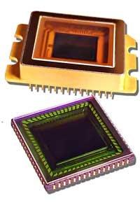
The uncooled FPA640x512_P15-C sensor (Badger-C) uses a simple, hermetic 64-pin ceramics LCC package with dimensions of only 18 mm x 18 mm x 2 mm and a sensor weight of just 1.7 g allowing a very compact and SWaP (Small Weight and Power) camera design. The power consumption is max. 200 mW as there is no cooler to drive.
The same InGaAs matrix sensor chip is now also available in a Kovar package with a 1-stage (FPA640x512_P15-TE1 = Badger-T1) or a 2-stage (FPA640x512_P15-TE2 = Badger-T2) thermoelectric cooler: these new cooled sensors utilize a high-quality 28-pin hermetic metal Shrink Dual Inline Package (SDIP) with a pin pitch of 1.78 mm, a size of only 36.1 mm x 25.4 mm x 6.3 mm (without pins) and a sensor weight of only 17 g. In the 2-stage cooled sensor housing, the chip is placed slightly higher, with the same housing dimensions.
In order to better adapt the sensor to an existing temperature control, the user can now choose between a cooler version with a high cooler voltage or a high cooler current (different cooler resistances). Also 2 different options of the integrated readout circuit are now selectable, which for the 3 possible sensor gain settings mainly differ from each other with regard to the conversion efficiency in μV / e- and the carrier capacity in e-.
The 2-stage cooled version is now also available with extended spectral range from 1.2 μm to 2.2 μm. All this gives the user a high degree of flexibility in adapting the image sensor or the camera to the target application.
Upon request ANDANTA can recommend a suitable socket to hold the sensors.
For further information please visit ANDANTA at LASER World of PHOTONICS 2019, Hall B3, Lounge „Made in Germany“ Booth 327/5, or visit ANDANTA’s website at www.andanta.de.
ANDANTA
Special image sensors for scientific applications. InGaAs-CMOS-Hybride, Si-CCD + CMOS – wissenschaftlich/scientific, Custom Si-TDI Komponenten/Components
ANDANTA GmbH
Ilzweg 7+9
82140 Olching
Telefon: +49 (8142) 41058-0
http://www.andanta.de
PR
Telefon: +49 (8142) 41058-0
E-Mail: Nadia.Sotiriou@andanta.de